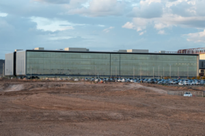
The rapid emergence of the “Silicon Desert” in north Phoenix has become one of the most transformative engineering and construction stories in the United States. Taiwan Semiconductor Manufacturing Company (TSMC) is developing what will ultimately be a massive multi‑fab semiconductor manufacturing cluster—a project now exceeding $165 billion in investment, making it one of the largest foreign direct investments in U.S. history. For professionals in the structural engineering and building envelope sectors, TSMC’s Phoenix campus presents a case study in scale, technical demand, and coordination across global supply chains. As the facility expands to support next‑generation chip production—including 4nm and 5nm in Fab 1, 3nm in Fab 2, and future 2nm and 1.6nm nodes in Fab 3 and beyond—the supporting architectural and structural systems must meet extraordinary performance requirements. In this Project Feature, we examine the broader context of the development and highlight Aquinas Engineering’s contribution to the building envelope systems that support this unparalleled industrial program.
Aquinas Engineering’s Contribution: Metal Panels, Louvers, and Shade Systems
Aquinas Engineering, in partnership with Kovach Enclosure Systems, is honored to contribute structural design expertise to this groundbreaking project through our work on metal panel systems, louvers, and shading assemblies. The metal panel systems used on the fabrication buildings must resist significant wind pressures, accommodate thermal expansion cycles, and integrate with complex sub‑girt support frameworks. Our engineering efforts focused on verifying panel attachment strategies, evaluating fasteners and anchors under critical load combinations, limiting deflections to maintain system integrity, and coordinating with manufacturer‑specific geometries and fabrication methods to ensure compliance with both project and code requirements.
In addition to the cladding, Aquinas Engineering – in partnership with Construction Specialties – provided structural calculations for the louvers and mechanical shading systems that are essential to regulating heat gain and protecting environmentally controlled interior spaces. Our engineering evaluations considered louver frame stiffness, blade spans, anchorage methods, and the combined effects of wind, seismic forces, and equipment‑generated loads. For the shading systems, we ensured that supports were structurally compatible with adjacent building frames and cladding elements, preserving both performance and constructability. These systems not only contribute to the functional performance of the semiconductor manufacturing environment but also enhance the architectural identity of the facility.
A New Epicenter for Semiconductors in the U.S.
TSMC’s decision to establish deep manufacturing roots in Phoenix aligns with the global push to diversify semiconductor production and enhance supply‑chain resilience. Fab 1 began limited production of 4nm and 5nm chips in 2024, serving major clients including Apple and NVIDIA. Fab 2 is now scheduled to enter 3nm mass production in 2027, accelerated from its original 2028 timeline. Further phases, including Fab 3, are expected to support 2nm and eventually 1.6nm nodes, pushing U.S. manufacturing capabilities into the realm of the world’s most advanced semiconductor technologies. Demand from domestic technology companies is heavily influencing these accelerated schedules. Apple alone plans to purchase more than 100 million chips from the Phoenix fabs by the end of 2026, reinforcing the strategic necessity of a U.S. production hub.
Project Scale and the Built Environment
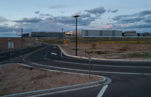
The scale of construction surrounding TSMC’s Phoenix campus is reshaping the region’s economic and physical landscape. TSMC recently expanded its land holdings by 902 acres, enabling long‑term development of up to six fabrication plants and an accompanying advanced packaging ecosystem, which includes domestic CoWoS capabilities essential for high‑performance AI processors. Since the initial development announcement, 39 semiconductor‑related companies have relocated to the Phoenix area, resulting in more than 7,700 new jobs and over $37 billion in additional investment, establishing the region as a growing national technology corridor. Surrounding development includes the 2,300‑acre Halo Vista project, a $7 billion mixed‑use environment designed to support industrial operations, research facilities, and residential communities linked to the Phoenix fabs.
For structural engineers—particularly those focused on curtain wall systems, metal panel assemblies, louvers, and other façade elements—this ecosystem presents unique challenges in performance, durability, and precision. Semiconductor fabrication environments require extreme environmental control, strict vibration standards, and envelope durability capable of withstanding the intense thermal fluctuations of Arizona’s desert climate.
The Workforce and Industry Impact
The Phoenix semiconductor build‑out is also transforming the regional engineering and construction workforce. TSMC has invested $5 million in apprenticeship programs that develop specialized fabrication technicians in partnership with Arizona State University, Northern Arizona University, Grand Canyon University, and Maricopa Community Colleges. Grand Canyon University has further supported this effort through an 11‑week semiconductor manufacturing program funded by TSMC and other partners, which has already placed 35 graduates into positions at the Phoenix fabs. This growth reflects a broader need within the semiconductor and microelectronics sectors for engineers and technical specialists capable of meeting the rigorous demands of advanced manufacturing infrastructure.
Looking Ahead: What TSMC Phoenix Means for Our Industry
As TSMC accelerates toward the production of 2nm process nodes and beyond, the supporting building systems—including structural, mechanical, and envelope assemblies—must evolve alongside these technological advancements. For firms specializing in building envelope systems, the Phoenix project represents a long‑term pipeline of sophisticated, performance‑driven work, with increasing emphasis on precision, reliability, thermal performance, and system integration. The ongoing development of this campus provides an opportunity for structural engineers to innovate, refine, and collaborate at a scale rarely seen in the industry.
Aquinas Engineering is proud to contribute to this historic effort through our structural work on metal panel systems, louvers, and shading assemblies. Our involvement reflects both our dedication to advancing building envelope engineering and our commitment to supporting the next generation of U.S. semiconductor manufacturing infrastructure.
Let’s build something extraordinary together.
📞 Contact us today: 210.237.7854
👉 Visit our website: https://aquinasengr.com/
📧 Email us at info@aquinasengineering.com
Photo Credit:
- https://restofworld.org/2024/tsmc-arizona-expansion/


Let us build a professional relationship. Tell us about your project today.
I really appreciated how quick and efficient the service was. It made our entire process much smoother. I’d just suggest continuing to maintain the quick turnaround, like getting the stamps within a day. It really helps us when we need them urgently, especially in situations where we might have missed the ball with our customers
Working with Aquinas has been nothing short of a pleasure. Not only are the response times great and consistent, Aquinas also provides strong and validating support above and beyond normal measures. I have zero criticisms. Aquinas Engineering has been an excellent asset to my team’s operation.
Quick fast service, great follow up. Aquinas approaches every project small and large with a high level of professionalism.